Better Thermal Management Improves Semiconductor Packaging
Advanced materials like SiC enable novel assembly methods needed for today’s thinner microelectronic components.
December 20, 2023 by Coherent

As microcircuits shrink, all the processes used to fabricate them must be retooled or replaced to work with smaller, thinner circuits and to deliver greater precision. This is especially true in “advanced packaging.” This is the production step where individual integrated circuits (called “dies”) are mounted and electrically connected to a substrate or circuit board, and then subsequently enclosed.
Flip Chip Basics
One widely employed advanced packaging technology is called “flip chip.” This method has become increasingly popular over the past decade because it offers several advantages over older methods like wire bonding. These benefits include lower cost, higher packaging density, and improved reliability.
To prepare circuits for flip chip, small bumps of conductive material – typically solder or gold – are first deposited onto conductive pads on the top surface of the semiconductor wafer. Then, the wafer is cut into individual chips (called die singulation).
Next, an individual die is picked up, turned so that the contact side faces down, and positioned over the substrate to which it is to be mounted. This substrate is most typically a printed circuit board. The chip is aligned very precisely so that the bumps on the chip match up with the corresponding conductive pads on the substrate (which are facing up). The chip bumps are brought into contact with the substrate pads.
This assembly is then put into an oven where it is heated above the melting point of solder (or whatever the bumps are composed of). The solder melts and “reflows” sticking to the conductive pads on both the die and the substrate. Finally, the oven then cools down and the solder solidifies to form both electrical and mechanical bonds between the chip and the substrate.
Thermal Compression Bonding – the Solution for Thin Dies
The flip chip process starts to run into problems as both ICs and substrates get thinner, and as the solder bump sizes and spacings between them (called the pitch) shrinks below 100 µm. Specifically, the heating cycle can cause warpage in the IC and substrate. This can occur due to temperature gradients across these components during the heating cycle and because of mismatches in the coefficient of thermal expansions (CTE) between various parts.
If part warpage is significant enough, then it can produce misalignment between the die and substrate. This can result in open circuits (no connection), or in some cases even short circuits (solder ball bridging).
Thermo-Compression Bonding (TCB) is a technology developed specifically to extend the capabilities of flip chip. Specifically, TCB provides a more reliable way to perform high-volume chip attach of thin dies.
The difference between traditional flip chip bonding and TCB is that the latter actively monitors and controls the temperature, exerted force, position, and orientation of the die and substrate during the entire operation with extremely high precision. Each step of the process is verified before moving on to the next. All this control results in better, more reliable bonds, and greater unit-to-unit consistency.
The main elements of the TCB system employed to accomplish all this are shown in the drawing. These include linear servo motors on air-bearing axes which can position the die vertically with a precision of 1 µm. There is also a tip-tilt stage for angular positioning to maintain co-planarity of the chip and die. Both a heater and cooler precisely control the temperature of the die, and the rate at which that temperature increases or decreases. The bottom of this stack of components is a vacuum chuck, or nozzle, which holds the die itself. And an array of sensors is embedded to continuously monitor the temperature, exerted force, position and orientation of the die and substrate during the entire operation.
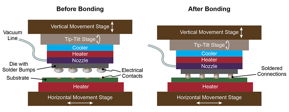
A thermal compression bonding system includes stages to position and orient the die and substrate, heaters and coolers to control their temperature, a vacuum nozzle to hold the die, and various transducers and vision systems (not shown) to monitor and control the process.
The TCB process starts out the same as traditional flip chip. Namely, a die is prepared with solder bumps. Then, the die is picked up, aligned with the substrate, and brought down until the bumps make contact with the substrate. After this, the heating and die movement cycle begins.
As the solder melts, the die is first moved towards the substrate, then slightly away from it, and then finally back towards it again. The temperature and exerted force are also varied, as well. All this ensures good alignment and bonding between the die and the substrate, uniform solder joint height, and a connection that is free from defects.
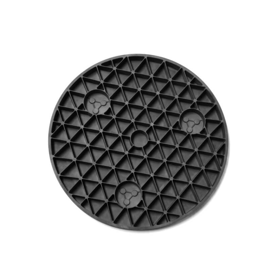
Coherent is a vertically integrated producer of materials and finished components for TCB nozzles. We can fabricate nozzles in a variety of sizes and shapes, and with internal features, such as this 4H SiC part.
Advanced Materials for Nozzles
Besides the stages, thermal devices, and sensors in the TCB system, another critical element is the nozzle. It serves three key functions. First, it contains various holes or channels for airflow allowing it to act as a vacuum chuck. Second, it maintains the flatness of the die throughout the process (because the vacuum holds the part securely against its surface). Finally, it conducts heat to allow the heating and cooling elements in the TCB system to vary the temperature of the die.
To meet these requirements, the ideal nozzle must be fabricated from a mechanically rigid material that can be made into parts that are both very smooth and flat. This is necessary to hold the die firmly and keep it flat throughout the process, even as the forces on it change.
Furthermore, the nozzle material must have high thermal conductivity. This ensures that temperature changes initiated by the heater and cooler are rapidly transmitted through to the die. The ability to precisely control the temperature of the die – and to quickly thermally cycle it – are key to the success of the process, and to minimizing its overall takt time.
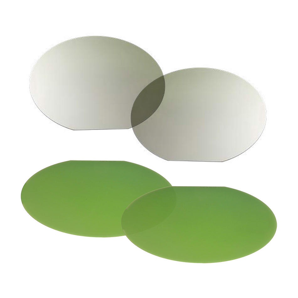
There are very few materials that meet all these requirements, but Coherent produces three different ones and can fabricate finished TCB nozzles from any of them. These are reaction-bonded silicon carbide (SiC), single-crystal SiC, and polycrystalline diamond. Each has its own specific characteristics and advantages, which are summarized in the table.
Material |
Thermal conductivity |
Surface Roughness |
Optically Transmissive |
Electrical Insulator |
Cost |
Reaction Bonded SiC |
255 W/m-K |
< 25 nm |
No |
No |
Low |
Single Crystal SiC |
370 W/m-K |
< 2 nm |
Yes |
4H: No 6H: Yes |
Medium |
Polycrystalline Diamond |
2200 W/m-K |
< 10 nm |
Yes |
Yes |
High |
All of these materials offer high thermal conductivity as compared with other substances – diamond has the highest thermal conductivity of any material. One key feature of reaction-bonded SiC is that it can readily be produced with whatever through holes or internal channels are needed. Also, it can be laser machined to achieve a very high degree of flatness and low surface roughness.
An advantage of both diamond and single-crystal SiC is that they are transmissive in the visible and near-infrared. This allows a wide range of measurement techniques to be used to measure flatness, thickness, and parallelism in the final part, thus enabling higher precision fabrication.
Polycrystalline diamond and 6H single crystal SiC are electrical insulators. This property can be useful for several reasons, including protecting the semiconductor die from damage due to electrostatic discharge (ESD).
There are also differences in the cost of nozzles fabricated from these three materials. This is important because nozzles are a consumable item that are periodically replaced.
Coherent is a vertically integrated manufacturer of TCB nozzles. We start by growing our own materials and go all the way through producing finished parts. A key component of our fabrication capabilities is our ability to produce very flat surfaces, and we have extensive metrology equipment to verify this flatness.
Learn more about reaction-bonded silicon carbide (SiC), single crystal SiC, and polycrystalline diamond from Coherent.