What are MicroLED displays?
In a few years, µLED displays will be a $10B-plus market. See why lasers play a critical role.
June 24, 2021 by Coherent
MicroLEDs (µLEDs) are a relatively new technology that produces brilliant, high-resolution displays that can be economically scaled up to huge dimensions – easily more than 20 feet (6 meters). Right now, they’re useful for large displays in conference rooms, arenas, concert venues, and outdoor applications. Eventually, they will probably become a common technology for big TVs. In the next five years, µLED displays will grow to be a $10B-plus market — and lasers play a critical role in enabling their production.
The difference between AMOLED and MicroLEDs
With AMOLED and other display technologies currently used for mobile devices and televisions, the light emitting (or light filtering) pixels are produced directly on the glass panel that forms the display. So, scaling them up in size means performing multiple steps with expensive OLED materials on a very large panel containing all the necessary circuitry. That gets expensive and impractical very fast as you go larger. It’s why televisions larger than 80 inches can cost tens of thousands of dollars.
MicroLED displays are different. The individual LED emitters are mass-produced on relatively small sapphire wafers. They are packed closely together resulting in low unit costs. These µLEDs are then removed from that wafer and transferred to a piece of glass with a circuit already patterned on it. Really huge displays can be cost-effectively constructed by increasing the spacing between the µLEDs on it – the main cost driver is then the number of pixels, not the size of the glass. Tiling together many individual panels also keeps costs down for larger displays.
Millions and millions of pixels
Now, there’s one big hitch. Each pixel in the µLED display consists of three separate LED emitters (red, green, and blue) which are really, really small. State-of-the-art is currently about 50 x 50 microns and is predicted to eventually approach 10 x 10 microns. And, there are literally millions of them. For example, even just a standard high-definition display (1920 x 1080) has over 2 million pixels. And, remember, each one of these pixels requires three separate µLEDs. So, a really large display might have 100s of millions of µLEDs in it.
The manufacturing challenge is to physically move all these tiny LED sources from the sapphire they’re grown on to the final glass display panel. And, to place them very precisely, and not to damage them. Any kind of mechanical method, whether it uses vacuum pickup or very precise actuators, would be too slow, and probably too rough, for handling the µLEDs. It should be no surprise that lasers supply exactly the “light touch” necessary for such a delicate and demanding operation.
What Is Laser-Induced Forward Transfer (LIFT)? Thanks for asking.
The practical method turns out to be a process called Laser-Induced Forward Transfer (LIFT). How does it work? You can see it illustrated in this video. In brief, it’s a two-stage process. First, the µLEDs are separated from the sapphire wafer they’re grown on and transferred to a temporary carrier using another laser-based technique called Laser Lift-Off (LLO). This leaves the µLEDs on the temporary carrier with the same close spacing they had on the growth wafer.
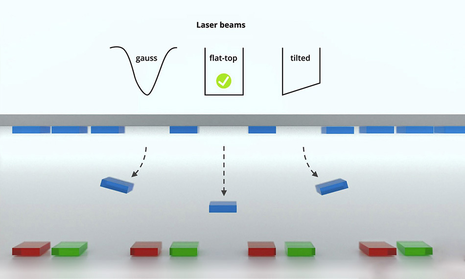
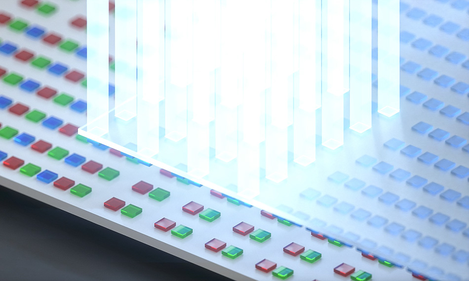
Figure. In LIFT a large area laser beam passes through a photomask so that only specific dies are released and pushed onto the display substrate. A uniform so-called top-hat beam is critical to perfect placement. (Not to scale).
Next comes LIFT. Here, pulses from an ultraviolet (excimer) laser enter through the backside of the carrier, which is transparent. The laser light is absorbed in the thin layer of adhesive which has been holding the µLEDs to the temporary carrier and vaporizes it. This actually physically blows the µLEDs off and pushes them onto the final display panel, which is placed in close contact. Adhesive on the final glass panel holds the µLEDs in place.
The beam and the mask
The secret is this, though. The rectangular laser beam passes through a mask that has holes in it that are the same distance apart as the pixels in the final display. So only every 5th, or even every 10th, µLED is pushed across to the display by a given laser pulse. The optical path with the mask is fixed and the temporary carrier then moved over very slightly to get to the adjacent set of µLEDs, but the display panel is moved a large distance, and the process is repeated on a new part of the panel. This allows a large number of µLEDs to be economically fabricated on a relatively small sapphire wafer and then placed with much larger separations to create a single big panel. And, the other big advantage of LIFT is that it’s fast. Thousands of µLEDs are moved by each pulse. At a laser pulse rate of 500 pulses/second (500 Hz), an area up to 32 mm x 1 meter can be covered in µLEDs in only a second!
We’re working on it
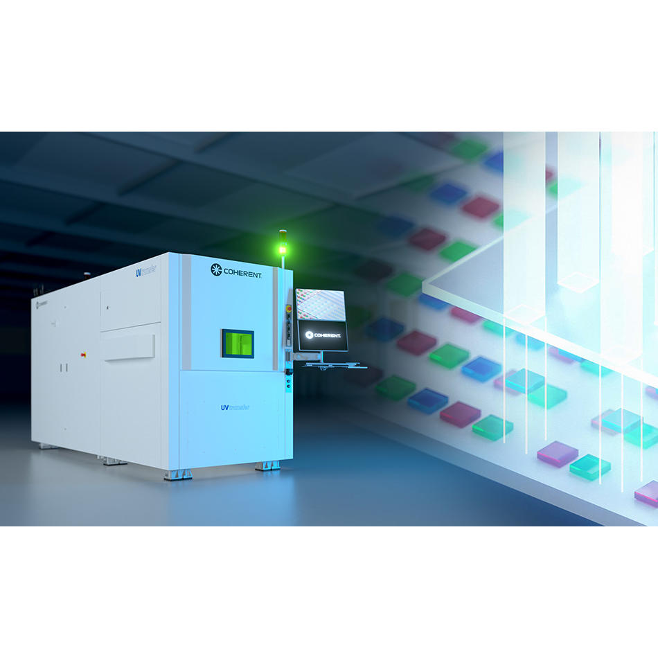
Coherent is already producing a tool called UVtransfer for µLED display processing that actually performs three separate processes – Laser Lift-Off (LLO), Laser-induced Forward Transfer (LIFT), and Repair/Trimming for defective pixels. This 3-in1 tool will set processing standards and demonstrates the potential of manufacturing large µLED displays practical and economical.
Related Resources