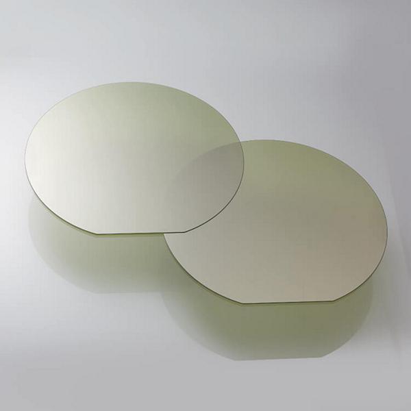
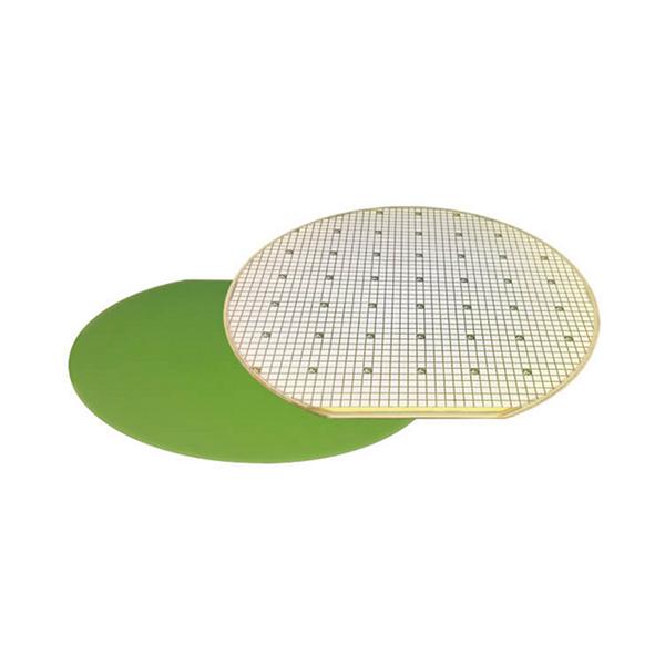
SiC Substrates & Epitaxy
SiC Epitaxy
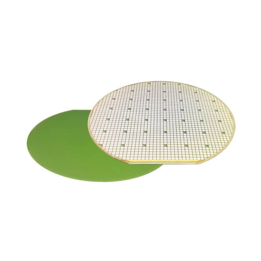
Accelerate time-to-market, reduce costs, and improve device performance by building on high-performance SiC epitaxial wafers from Coherent in up to 200 mm diameter.
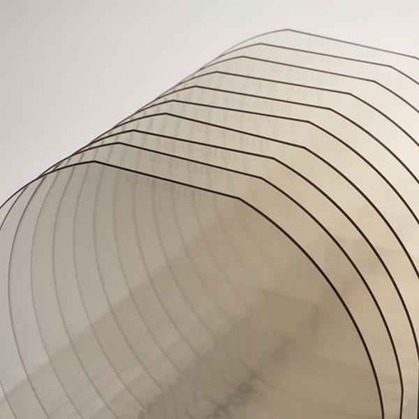
Coherent offers a total SiC materials solution with options for thick epilayers with or without buffer, low-doped layers, multilayer structures, p-n junctions, embedded/buried structures and contact layers, and more. We support R&D to volume production.
SiC Epitaxy Capabilities Highlights
State-of-the-art SiC epitaxy technology
Record-low defect density through efficient buffer-layer technology
Prevents nucleation of crystalline defects at growth start
BPD to TED conversion rate >99.8% → 1 BPD per cm2
Enables bipolar SiC device technology
Best-in-class layer homogeneity
Adjustable lateral gas flows
High growth rate of 40 µm/h using TCS as a silicon precursor
Thick layer growth of 150 µm and more
Low doping concentrations of 1×10¹⁴/cm3
Enables >15 kV SiC device technology