Semiconductor Equipment
World-class solutions and service
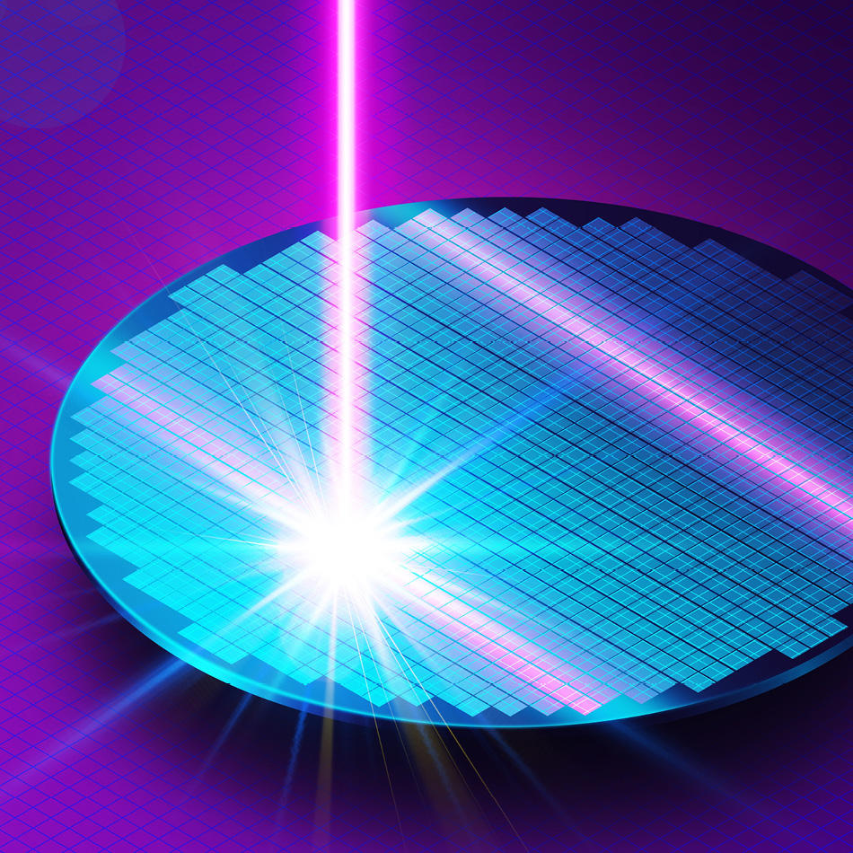
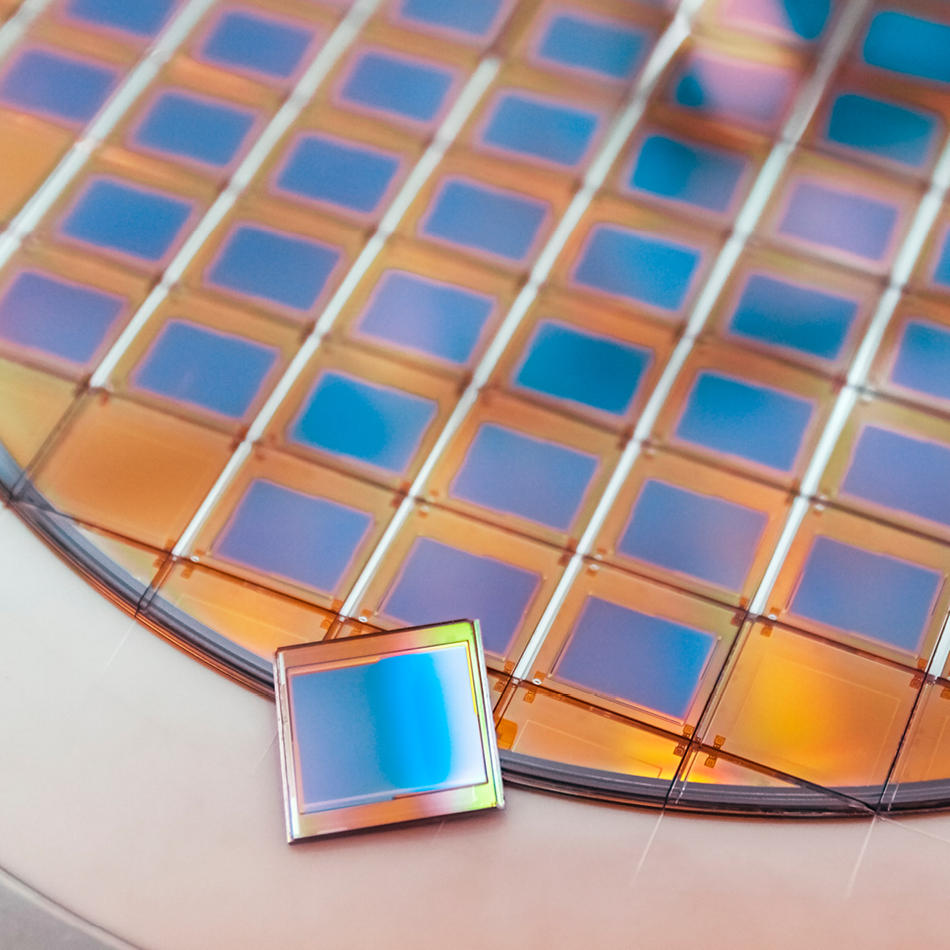
Build manufacturing and testing equipment with the speed and accuracy needed for advanced chips and next-generation packaging.

More Featured Assets

Ready to Get Started?
Share your contact info and a specialist will reach out.
Shop Coherent
Online shopping for lasers, optical fibers, power meters and sensors, accessories, and much more on Coherent online has never been easier.