LASERS SAVE MICROLED DISPLAYS – AGAIN
Laser-assisted bonding bypasses one of the remaining roadblocks in volume microLED display production.
March 28, 2024 by Coherent
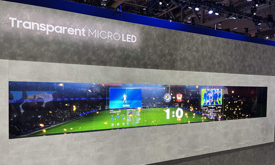
Samsung wowed attendees at the Consumer Electronics Show (CES) in January 2024, with their huge, transparent microLED display. But there’s more to microLED displays than just good looks. They offer several advantages over other display technologies, such as LEDs and OLEDs. These include improved energy efficiency, longer lifetimes, higher brightness, and better color accuracy. In addition, utilizing microLEDs allows manufacturers to easily modify size, shape, and resolution to create new display designs without the need for extensive retooling.
Despite these advantages, microLEDs have yet to become commonplace. This is because they are generally more complicated to make than other displays. There are still some significant challenges that must be overcome for successful commercialization of this technology.
Excimer Lasers Give microLEDs a LIFT
To help understand where these challenges occur, the drawing illustrates some of the key steps in microLED display production. After these are completed, there are various other testing steps and an “aging” process. Large displays are made by combining multiple smaller panels, so additional assembly and packaging steps occur if this is the case.
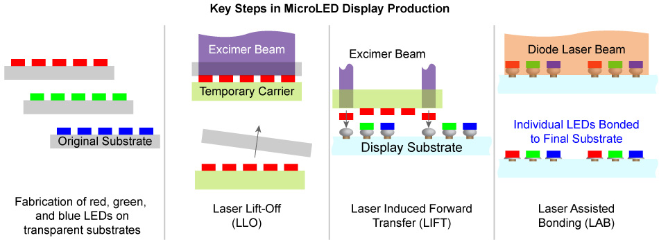
1) Red, green, and blue LEDs are separately fabricated on transparent substrates. 2) LLO: The LEDs are contacted to a temporary carrier which has adhesive to hold them. An excimer laser is focused through the transparent substrate and separates the LEDs from it. 3) LIFT: An excimer laser is focused through the temporary carrier to separate the individual LEDs and propel them towards solder pads on the final substrate. 4) LAB: A diode laser heats numerous LEDs and solder bumps at once to rapidly melt them and form a final bond.
Like most semiconductor devices, LEDs are originally epitaxially grown on a wafer. Typically, this is a sapphire substrate. Separate LEDs that emit at each of the primary colors – red, green, and blue – are required to make each pixel of a microLED display. But each wafer only contains devices of a single color. So, the LEDs must be separated into individual dies, and then arranged together in the necessary pattern to make the final display.
Excimer lasers have already proven themselves as cost-effective tools for the first two major steps in this process. Specifically, Laser Lift-Off (LLO) is used first to separate the individual LED dies from the sapphire wafer and transfer them to a temporary carrier.
Next, Laser Induced Forward Transfer (LIFT) is used to perform ‘mass transfer.’ This is the process of moving the dies from the temporary carrier to the final display substrate. Most importantly, mass transfer is where the LEDs are arranged into the desired pixel pattern.
The microLED Assembly Challenge
After the LEDs are in place on the substrate, they must be bonded and electrically connected to it. Otherwise, the display wouldn’t light up, and all the LEDs would just fall off it when it was moved!
To facilitate this process, solder ‘bumps’ (small balls of solder) are first placed on the substrate at all the intended points of electrical connection. Then, after die placement using LIFT, the solder is heated until it melts. It flows around the electrical contacts on both substrate and die in this state. It subsequently cools and resolidifies forming both an electrical and mechanical connection between them. This is a standard assembly technique throughout the electronics industry.
The most common method for melting the solder is called ‘mass reflow’ (MR). It essentially involves placing the entire assembly of substrate containing solder balls and dies into an oven. The temperature is cycled to melt the solder and then it to cool back down.
But mass reflow can’t help microLED manufacturers make the jump to smaller LEDs which must be placed closer together with higher positional accuracy. The problem is that the heating cycle takes several minutes. This produces a substantial heat load on all the components and can warp components, introduce thermo-mechanical strain, and physically shift the position of the dies on the substrate. The long process time in the mass reflow oven also increases the risk of making bad electrical connections. The process itself is also energy-intensive.
Thermal compression bonding (TCB) is an alternative that reduces the risk of warping caused by the MR. TCB adds force while the heat applied which better controls the height and shape of the interconnections. But it does require a complex nozzle which is customized for the specific die and package body size, and essentially only bonds a single die at a time. This makes it less suitable for microLED applications which can require bonding literally millions of LED dies to make a single display.
Laser-Assisted Bonding
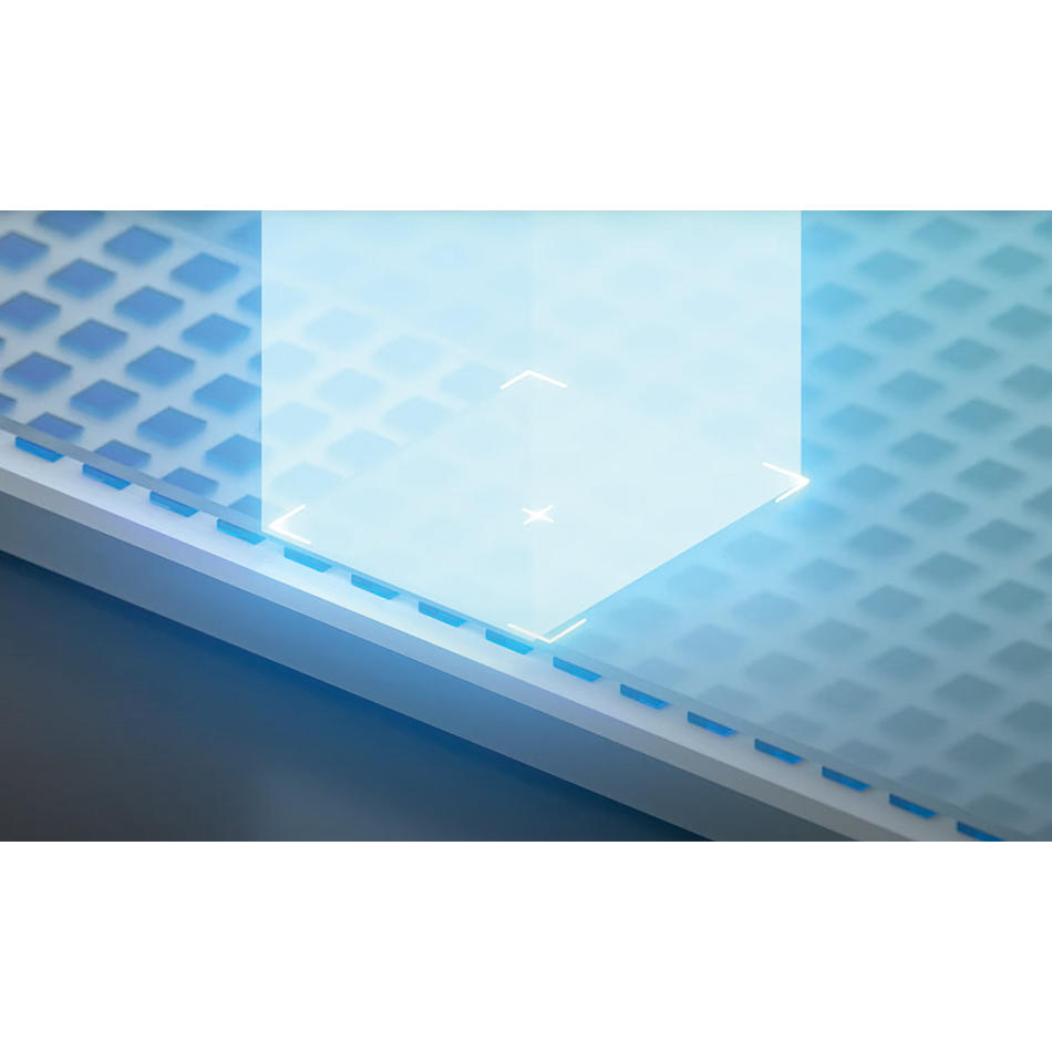
Laser-assisted bonding (LAB) addresses all these issues. In LAB, the output of a high-power, infrared diode laser beam is shaped into a rectangle. The intensity distribution is homogenized to be highly uniform over the entire area of the beam. The dimensions of the rectangular beam vary by application. but it’s quite possible to make it large enough to illuminate thousands or even millions of LEDs on the substrate at once.
During LAB, the laser is turned on very briefly – for less than one second. But this is sufficient time to transfer enough heat into the assembly to melt the solder. However, it is too short to cause any significant bulk heating that would lead to warpage or positional shifting of the dies. The laser enables precise control of the heating cycle, with cooling phases included as necessary. As a result, the soldering process is performed quickly and without any significant negative consequences. The brief cycle time of LAB also makes it substantially more energy efficient than either MR or TCB.
Better Lasers for Improved LAB
In terms of the laser, a critical requirement for LAB is that the beam intensity be uniform over its entire area. This is necessary to achieve consistent, uniform heating of the solder and therefore consistent results. The goal is to selectively heat only the desired area – containing a specific number of microLED – and not to heat surrounding areas at all. This makes it particularly important to produce a rectangular beam pattern where the intensity doesn’t fall off much near the edges. Otherwise, it’s possible that the LEDs in this region won’t get bonded at all. But the beam intensity must drop off very rapidly outside of the area being illuminated.
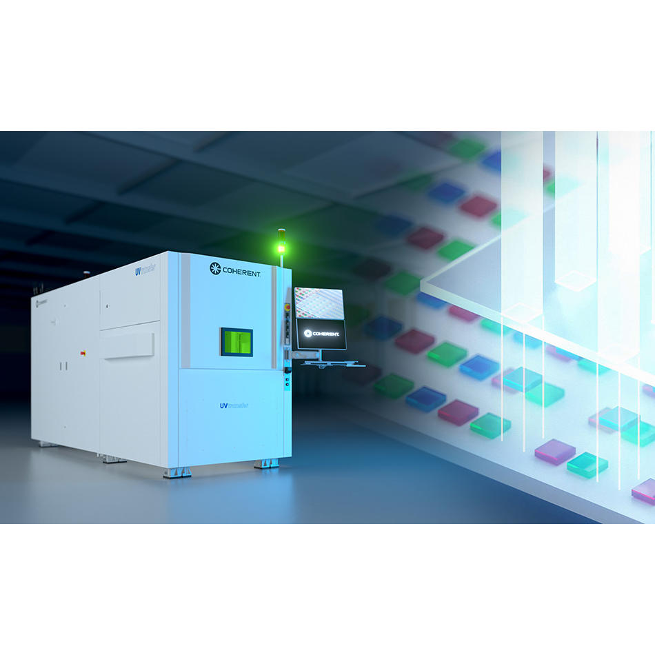
The Coherent HighLight DL series of fiber-delivered diode lasers can be paired with our PH50 DL Zoom Optic to produce exactly this kind of highly uniform rectangular beam. Typically, a 4 kW HighLight DL laser (between 1 – 4 kW) is used for LAB of microLEDs.
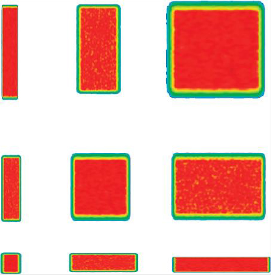
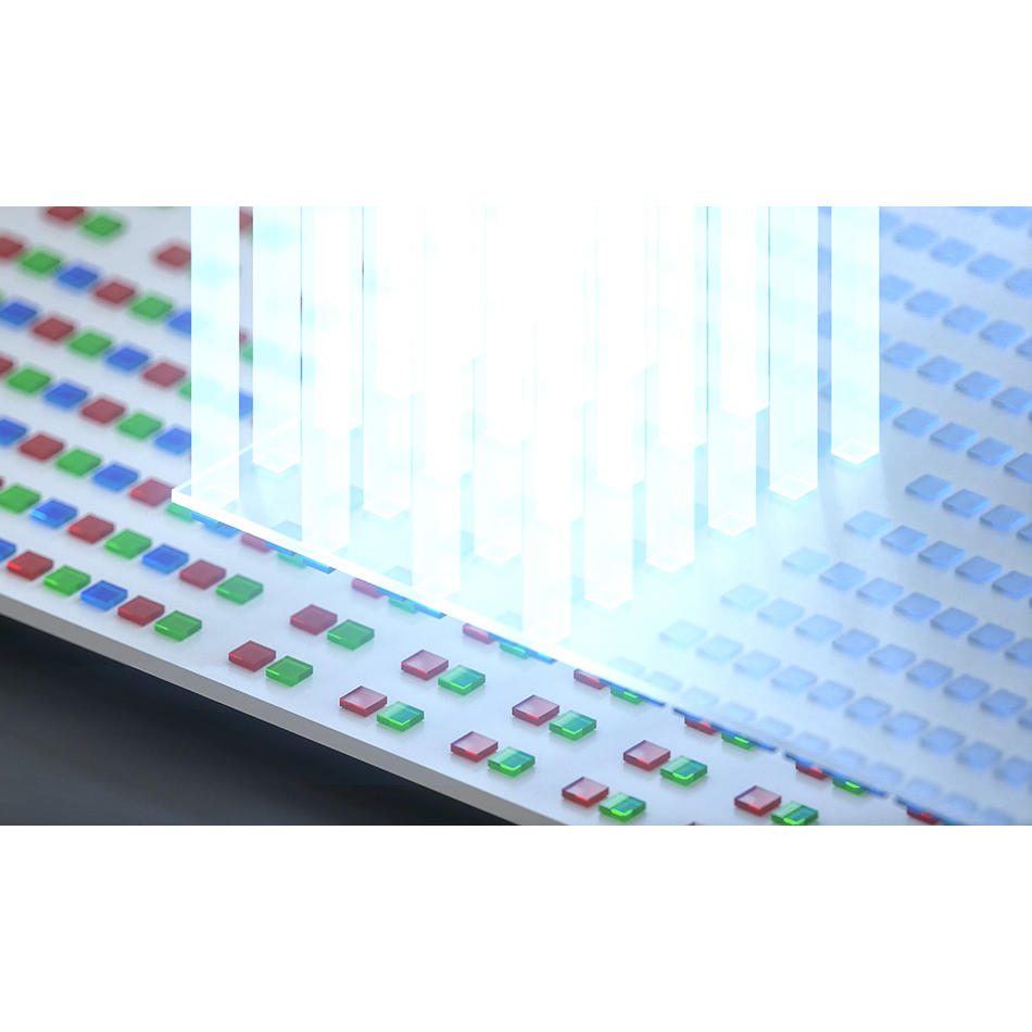
The Coherent PH50 DL Zoom Optic transforms the fiber-delivered, multi-mode output of a HighLight DD series diode laser into a highly uniform rectangular beam. The length and width of this rectangular can be independently adjusted dynamically. The spot sizes shown here range from 12x12mm to 110x110mm, but other zoom configurations are available.
This combination delivers better intensity uniformity than available from any competitive products by using our own proprietary optical design. Specifically, the beam homogenization is accomplished using an array of micro lenses to separate the incoming laser beam into numerous ‘beamlets.’ These are then expanded and overlapped to yield a highly uniform intensity distribution.
Another big advantage of the Coherent PH50 DL Zoom Optic is that it is adjustable ‘on-the-fly,’ even during the process, Namely, both the length and width of the rectangular beam can be independently adjusted over a wide range as needed. This zoom capability is useful to manufacturers as they develop and qualify their process. It enables them to try various configurations to see what works best and most efficiently. Of course, Coherent can utilize the same approach to produce fixed (not zoom) optics that meet specific customer requirements. Such line beams can range from a few millimeters up to 1000 mm.
LLO and LIFT are already established as two key enabling technologies in microLED production. Now it looks like another process based on a Coherent laser – LAB – will facilitate the manufacture of high-resolution microLED displays in volume.
Learn more about Coherent lasers for LAB.