Lasers in Display Fabrication: MicroLED Lift-Off, Transfer, and Repair
Coherent UVtransfer systems perform three critical steps in the production of MicroLED displays resulting in scalable displays with stunning resolution and brightness.
October 4, 2022 by Coherent
In this sixth installment of our series on flat panel display manufacturing, we’ll look toward the future and see how lasers enable the automated volume production of next-generation displays based on MicroLEDs.
AMOLED technology now gives us thin displays for smartphones and TVs with fabulous colors and resolution. But display manufacturers are already progressing towards volume production of the next “big thing” in displays: MicroLED displays.
Read the other blogs in this series on lasers in display fabrication |
|||
Based on small (<50 micron) inorganic LEDs this fast-emerging technology promises several advantages. First, it is immune to premature aging which can sometimes affect OLED emitters. In addition, it can deliver higher brightness with higher contrast. In addition, it is a scalable technology with the potential for producing large TVs and public displays at a more economical price point as well as ultra-compact displays for VR/AR applications.
MicroLED displays have actually been around for a while in limited volume but now display manufacturers are figuring out how to take this into full-blown production. It turns out that lasers are playing several critical roles. Let’s take a look
Wafer-scale economy
Inorganic (semiconductor) LEDs support high light output – witness their use in high-brightness automotive headlamps. This allows MicroLEDs to be really small but at the same time very bright. State-of-the-art size is currently about 50 x 50 microns and is predicted to eventually approach 10 x 10 microns.
There are three kinds of these active emitters: red, green, and blue. Each type is mass-produced (by epitaxial growth) on a densely patterned sapphire wafer. So a 6-inch diameter wafer can be patterned with many millions of individual MicroLEDs, providing volume of scale economics.
These are eventually placed on a large relatively inexpensive piece of glass with the necessary circuitry to function as a thin display. In a large display consisting of several separate tiles, the total display area might be two meters across, and the pixel pitch might be a millimeter or more. Even with three of the tiny emitters in each pixel site, most of the display is dead space. For large-size scaling, this means that the major cost driver is the number of pixels, hence the promise of eventual lower costs.
While the concept is straightforward, the practical implementation is definitely not!
Getting Lift-Off
Actually there’s a big overarching challenge to making all this work. Millions of these MicroLEDs (dies) have to be moved from the sapphire wafer on which they are created and precisely placed on the large display panel. Believe it or not, in some early prototypes the individual dies were mechanically picked up and placed, e.g., by vacuum robotics. But that’s just too slow for final production. And as the dies get even smaller, it’s hard to do this quickly without the risk of damaging some of them during handling. Yields have to be very high because of the incredibly high volume – for an 8K display, we’re talking about over 30 million pixels, i.e., almost 100 million dies.
The solution is to use lasers in automated multiplex processes related to some of the well-proven techniques described in earlier documents in this series.
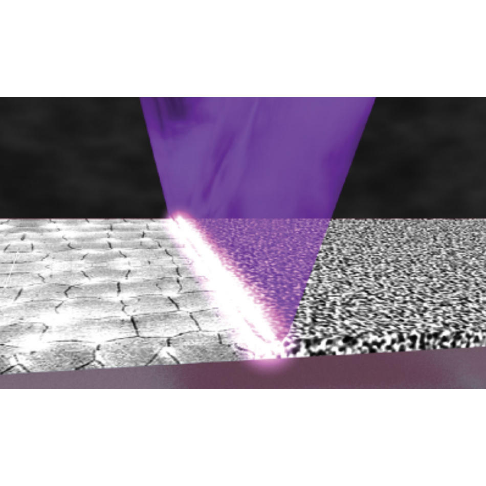
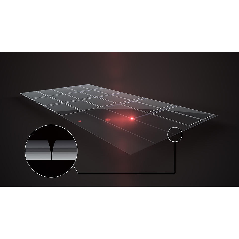
There are actually three separate processes involved: lift-off, transfer, and repair. First, the MicroLEDs are separated from the sapphire wafer they’re grown on and transferred to a temporary carrier for easy handling using a conventional laser-based technique called Laser Lift-Off (LLO). The carrier is coated in an adhesive and brought into contact with the tops of the dies. Ultraviolet light from an excimer laser is directed from behind the sapphire wafer, vaporizing a thin sacrificial layer of material that was deposited on the wafer before the dies were formed. This leaves the MicroLEDs on the temporary carrier with the same close spacing they had on the growth wafer.
LIFT – changing the pitch
Next comes Laser-Induced Forward Transfer (LIFT). Here, pulses from an ultraviolet (excimer) laser enter through the back side of the carrier, which is transparent. The laser light passes the carrier and the adhesive and interacts with the remaining buffer layer of the GaN. This delivers a transfer with almost no residues and no impact on the MicroLED customer-facing surface if short UV wavelengths is used! This physically blows the dies off and pushes them onto the final display panel, which is placed in close contact but with a certain gap which has to be larger than the thickness of the MicroLED´s to avoid collisions. Adhesive on the final glass panel holds the MicroLEDs in place.
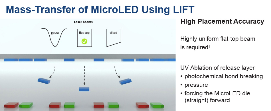
In LIFT a large area laser beam passes through a photomask so that only specific dies are released and pushed onto the display substrate. A uniform so-called flat-top beam is critical to perfect placement. (Not to scale).
Now comes the critical piece of “magic,” the change in the pitch (die spacing). The rectangular laser beam passes through a mask that has holes in it. The beam is then demagnified 2.5X or 5X so that the projected pattern of holes are the same distance apart as the pixels in the final display. In this way, only every 5th, or even every 10th, or any other integral multiple of the LED pitch on the EpiWafer, is pushed across a tiny gap of a few micrometer to the display by a given laser pulse. The carrier is then moved over very slightly MicroLED relative to the fixed beam and mask to get to the adjacent set of MicroLEDs. The display panel is moved a larger distance, and the process is repeated. Don’t worry if this step and repeat sounds a bit confusing; we have a great video that makes it pretty simple to understand.
Alternatively, some manufacturers are working on a slightly different sequence where the pitch is changed as the dies are lifted off the EpiWafer. This is called selective LLO. But the overall result is the same.
High throughput and repair
LIFT allows a large number of MicroLEDs to be economically fabricated on a relatively small sapphire wafer, and then placed with much larger separations (pitch) to create a single big panel. And the other big advantage of LIFT is that it’s fast. Thousands of MicroLEDs are moved by each pulse.
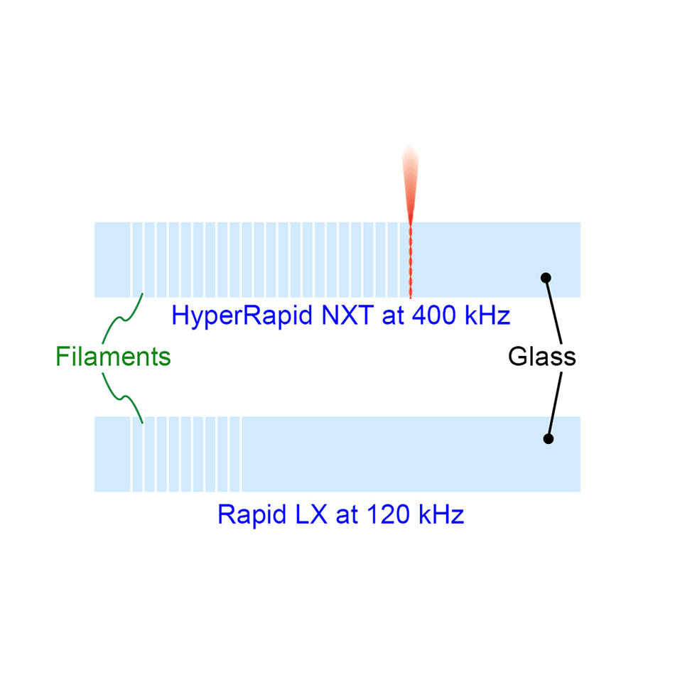
In the current R&D targeted implementation, the excimer laser pulse rate is up to 20 pulses/second (20 Hz), meaning an area up to 640 mm2 can be covered in MicroLEDs in only a second! But this excimer laser technology is extremely power scalable as demonstrated in annealing applications which uses high (over 1 J) pulse energies and high repetition rates. In LIFT, higher pulse energies can be exploited to enable larger masks and field sizes.
Now the yields for making relatively simple semiconductor devices like inorganic MicroLEDs are incredibly high. But there’s millions of them on each display, so there’s a small but finite possibility of a defective or mishandled pixel meaning one of the RGB devices is not emitting correctly. That’s easy to repair in an automated laser process by adding a replacement die using a mask with a single hole in it or a scanner-based system.
Coherent is already supplying a tool called UVtransfer for MicroLED display production that actually performs all three of these processes – Laser Lift-Off (LLO), Laser-induced Forward Transfer (LIFT), and Repair/Trimming for defective pixels. This 3-in-1 tool will make production of large MicroLED displays practical and economical.
Learn more about Coherent UVtransfer systems.