ホワイトペーパー
MicroLED - ディスプレイ製造用レーザプロセス
概要
高エネルギーの紫外線レーザビームにより、特にレーザリフトオフ(LLO)、レーザ誘起前方転写(LIFT)、ピクセル修復などの、ディスプレイ製造のためのUVtransferプロセスが可能になります。 このドキュメントでは、ダイの小型化が進む中で、こうした大量移載・配置の生産工程がUVtransferによってどのように将来性を確保できるのかを始めとして、最新の情報をお伝えします。 さらに、この加工方法にはさまざまな修復方式に対応できるという長所があり、期待通りのダイ歩留まりが得られます。
MicroLEDの可能性と課題
MicroLED(μLED)は、未来のディスプレイに大きな可能性をもたらす、新しいタイプのデバイスです。 一般的に窒化ガリウム(GaN)をベースとしており、現状では寸法が20~50 µm程度ですが、将来的には10 µm以下まで小型化されると予想されています。 サファイア成長ウエハの基板に既存のGaN製造技術を駆使することにより、数ミクロンの線幅で非常に高い密度を達成できます。
ミクロンサイズの寸法、高輝度、高製造密度を実現したことで、ディスプレイ市場は有機ELや液晶ディスプレイにより拡大を遂げた現在の市場を超えてさらに拡大することでしょう。 たとえばμLEDは、1インチ未満の超小型AR/VRアプリケーション用高解像度ディスプレイの製造に使用できます。 サイズとしては正反対ですが、屋内・屋外用の大画面ディスプレイにも対応しています。
ダイサイズが小さくなればなるほど、ウエハ上に形成できるダイの数が大幅に増えるため、このような大型ディスプレイはμLEDから経済的に製造することができます。その結果、大型ディスプレイではピクセルのピッチがダイの寸法よりもかなり大きいため、メインディスプレイのコストドライバーはピクセルの合計数になります。 これは、コストがディスプレイ面積に連動する有機ELなどの技術とは対照的です。
ただし、μLEDが広く導入されるには、克服すべき技術的課題がいくつかあります。 その1つが、サファイアウエハの成長基板からダイを分離するプロセスの開発です。 ほかにも、ミクロンレベルの精度と信頼性でディスプレイ基板にダイを移載するプロセスがあります。 こうしたプロセスは、不良ダイという避けられない問題に対処するための修復・交換方式と互換性を持つ必要があります。 同時に自動化にも対応し、LED産業が現在の総コストにおいて最大20倍のコスト削減を目指す中で、高スループットを実現する必要があります。 また、ダイは今後も小型化することが予想されるため、サイズを小さくするたびに多額の資金が必要となる設備の入れ替えをしなくても小型化のトレンドに対応できるようなプロセスが望ましいでしょう。
「ダイの小型化の継続により、小型化のトレンドに対応できるようなプロセスが望まれます。」
図1 : 直視型の大型MicroLEDディスプレイの図
レーザ加工のコンテキスト
高エネルギー紫外線レーザパルスおよびナノ秒パルス幅によるレーザ加工には、こうした課題に対応できる独自の利点があります。 短波長UV光は、材料の薄層に直接働いて界面や表面で剥離し、材料に深く浸透することはありません。 このコールドフォトアブレーションプロセスと短パルス幅を組み合わせ、下層の材料への熱による衝撃や損傷を防ぎます。 また、パルスエネルギーが大きく、ビームをフォトマスクに照射して1回のパルス照射で何百、何千ものダイを加工できるため、並列処理が可能になるという、ほかにはない利点もあります。 そのため、有機ELおよび高性能液晶ディスプレイのTFTシリコンバックプレーンを製造する大量生産ツールとして、このようなタイプのレーザがディスプレイ業界に浸透しており、次世代のμLEDディスプレイでももちろんそれが続くでしょう。
このときレーザ加工は、いくつかの点でμLEDディスプレイ製造に貢献します。
- レーザリフトオフ(LLO)により、完成したμLEDをサファイアウエハの成長基板から分離
- レーザ誘起前方転写(LIFT)により、μLEDをドナーから基板へ移載
- μLEDによるレーザ修復で、歩留まりの問題や不良率に対処
- エキシマレーザアニーリング(ELA)により、LTPS-TFTバックプレーンを製造
- さまざまな積層レベルでのレーザ切断に対応
これらの分野における最近の主な進展を以下に示します。
レーザリフトオフ(LLO)に関する最新情報
完成したμLEDをサファイアウエハの成長基板から分離するレーザリフトオフ(LLO)については、以前Micro-LEDのレーザ加工で説明しています。 そのためここでは、現在開発途上のツールである最新の自動アライメント機能を含め、青色や緑色のダイのLLOに関する主な改善点について、簡単に紹介するにとどめます。
バルクGaN μLEDは通常、最適な成長基板であるサファイアの上に形成されます。 しかし垂直構造のLEDが動作するための2つ目の接点を作るには、薄膜LEDをサファイアから剥がさなくてはなりません。 また、サファイアはμLEDダイの50~100倍の厚みがあり、下流で加工するにはかさばりすぎます。 そのため、高密度のμLEDをサファイア基板から一時的なキャリアに移載する必要が出てきます。
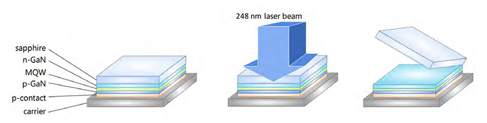
図2: GaN膜をサファイアウエハから剥離するLLOプロセスの概要
μLEDのLLO用として、CoherentはUV転写プロセスを開発しました。 LLOプロセスでは、背面から(透明サファイアを通過して)ダイに照射します。 これによりGaNの微細な層が浸食され、少量の窒素ガスが発生してダイを分離します。 波長(248 nm)のUVtransferプロセスは、AlNなどほかの類似材料で成長させたμLEDにも使用できます。
UVtransferプロセスでは、UVレーザビームをトップハット型の出力プロファイルを持つ方形にしてから、フォトマスクを通してサファイアウエハに照射します。 この均一な強度によって、加工フィールド内のあらゆるポイントに同一の力が加えられます。 光学系は、高エネルギーパルスごとに大きな面積のダイをリフトできるよう設定されています。 この並列処理ができるという長所は、高エネルギーのUVエキシマレーザパルスをベースにしたUVtransferプロセスを使用する当社のLLO特有のものであり、大量生産でコスト削減を実現するための重要な要因となります。 (Coherentの類似システムであるUVbladeは、柔軟な有機ELのLLOに広く使われています)。
エキシマレーザベースのLLOシステムは、μLEDのパイロット生産ラインのいくつかですでに稼働しています。 照射(マスク)されたビームに対するウエハの動作は、当初は並進ステージ上のエンコーダーだけで制御されていました。 最近の進歩である「ダイ上加工」はUVtransferプロセスの核となる機能で、アライメントの精度をさらに向上し、ダイを小型化しストリートを狭めることに役立っています。
また「ダイ上加工」によって、レーザラインの端にあるダイへの照射が部分的になってしまう可能性がなくなります。 この場合大まかなアライメントは、やはり並進ステージ上のエンコーダーで監視されています。 しかし詳細なアライメントは、閉ループのスマートビジョンシステムで行われ、ダイの碁盤の目状の並びを利用して、ビームに対してウエハの位置が合わせられます。 これにより、レーザフィールドの端が常にストリートの中央に来て、ダイを横切ることはありません。
図3: 図3. UVtransferプロセスでは、ダイ上加工機能により、レーザフィールドの端が常にストリートの中央に来ます。
レーザ誘起前方転写(LIFT)
UVtransferプロセスはまた、レーザ誘起前方転写(LIFT)の原理を使って、選択したダイを大量移載・配置するのに最適です。 ここで重要な課題となるのが、ピッチの劇的な違いです。 ウエハと移載キャリアの上に、現在は約1000 dpiのピッチで緊密にダイが並べられています。 しかしサイズや解像度によって、ディスプレイ上のピッチが50~100 dpiしかない場合もあります。 また、ダイは順番に配置し、赤、青、緑を各ピクセル位置に置く必要があります。
レーザ以外の既存の移載方法では、必要な解像度で必要なスループットを実現できません。 たとえば、機械的なピックアンドプレース方式では速度と配置の精度に限界があるため、現在のテクノロジーの方向性には対応できません。 一方、フリップチップボンダーは高精度の配置(±1.5 μm)を実現していますが、一度に1つのダイしか処理できません。 対照的に、UVtransferは高精度(±1.5 μm)および大量の並列処理をする能力があり、何千ものダイを1回のレーザ照射で移載・配置できます。
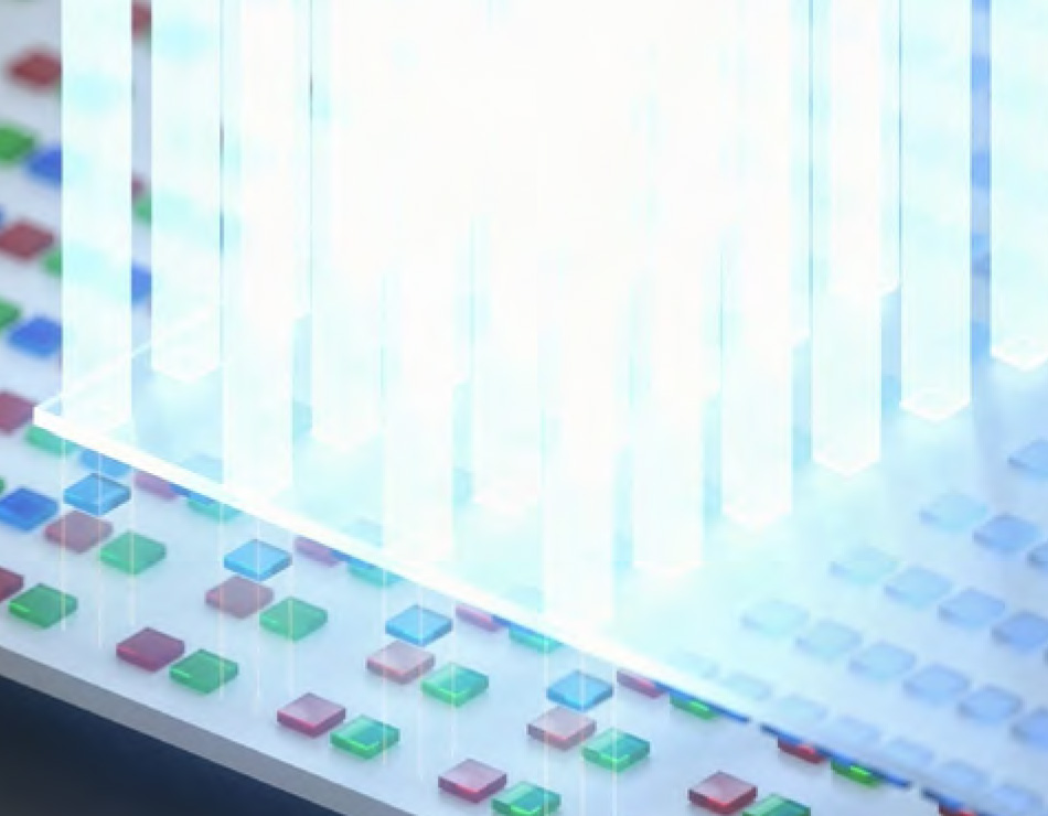
図4は、この方式の仕組みを図で表しています。 LLOは、動的分離層を使って一時的なキャリアにダイを付着させたままにします。 これは、UV光を非常に吸収しやすい無害な接着剤です。 一時的なキャリアとダイは、最終的な基板と近接して配置されます。最終的な基板は通常、ガラスか柔軟なパネルにTFTバックプレーンを事前に形成し、接着層またはパッドを被せたものです。 UV光はキャリアの背面から照射されます。 実質的にすべてのレーザエネルギーが動的分離層に吸収され、動的分離層は気化します。 膨張した気体の圧力による衝撃で、キャリアから最終的な基板上にダイが押し出されます。理想的には、ダイに残留物は残りません。
図 4: UVtransferがマスクを使ってステップアンドスキャンプロセスを実行し、ディスプレイ上に正しいピッチを形成。
エリア全体の隣接ダイを同時に処理するLLOプロセスとは異なり、移載プロセスでは、ダイの間隔が、元のウエハの近接した間隔から、最終的なディスプレイのピクセル間隔に変わります。 これは、たとえば5番目ごとや10番目ごとにダイに照射するようなパターンのフォトマスクを使って行われます。 ディスプレイの次のエリアがダイを乗せる位置に並進すると、1単位分のウエハ間隔を移動するよう、マスクの割り出しが一時的なキャリアに対して行われ、まったく新しい配列のダイが移載されます。
LLOと移載のもう1つの違いは、後者には接着剤の剥離が含まれ、必要なレーザフルエンスがIII-V族半導体の5~20倍低いことです。 この高効率性は、レーザ出力が低くても高スループットが得られることを意味しています。
UVtransferプロセスは、実装時にも重要な特徴があります。 たとえば、キャリアにマウントされたダイとTFT基板の間に隙間がほぼない場合でも、損傷なく正確な配置で各ダイの移載を成功させるには、衝撃の力を管理・制御する必要があります。 特に、力の大きさと方向をディスプレイ全体に最適かつ一定のものにし、移載の処理ウィンドウを確保できるようにします。
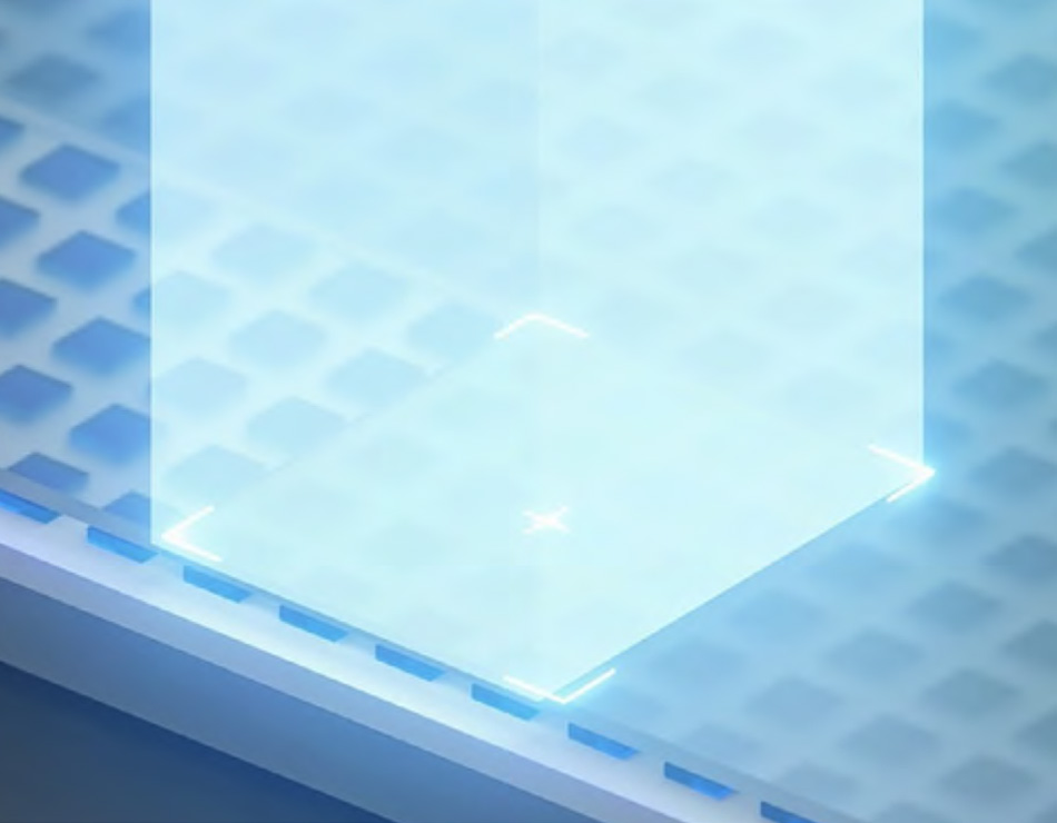
処理フィールドのダイに対して極めて均質で一定した移載を行うには、極めて均質なレーザ照射が必要です。これはCoherentのコアコンピテンシーであり、さまざまな用途で広く利用されています。 これにより極めて均質な2Dフィールドができ、用途に応じて正方形や高アスペクト比の長方形に形が変えられます。 たとえば6インチのウエハーの移載では、ウエハーの有効フィールドは約100mm x 100mmです。図4にあるように、局所(1つのダイ)に対する強度が均一ということは、エリアのどこでもダイが均等に押し出されることを意味します。 つまり、力は常に垂直方向で、ガウス型または傾斜型の強度プロファイルを持つビームが引き起こすような、横方向のずれはありません。 大きな範囲(ウエハ幅)のビーム強度が均質であることも重要です。それにより、各ダイが同じ力の大きさで押し出されます。
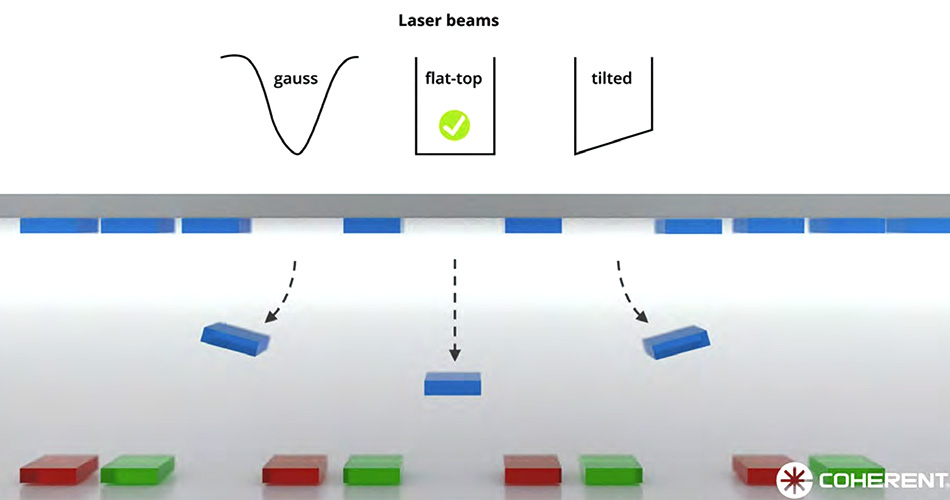
図5 : 正確な配置には、極めて均一な「フラットトップ」ビームプロファイルが不可欠(正確な縮尺ではありません)
重要なのは、UVtransferプロセスが、極めて小さなダイ(5ミクロン未満)や、現在のパイロット生産より狭いストリートに簡単に対応できる点です。 実際、短波長UV光によって、将来のミクロンレベルの解像度が実現可能です。 ダイの小型化に必要なのは、異なる照射マスクだけと言えます。
赤色ダイの修復・交換
μLEDベースのディスプレイが市場で成功するには、製造コストを大幅に削減し、歩留まりを100%に押し上げる必要があります。 これが達成できない場合、何億ピクセルにもなり得るディスプレイは実用化できません。 しかし不良ダイは避けられないため、メーカーができるのは、さまざまな修復・交換方式と互換性のある製造技術プラットフォームを採用することしかありません。 LLOと移載の両方に適用した場合のCoherentのUVtransferは、すでに研究されている交換方式と互換性があります。
このプロセスの最初のステップでは、不良ダイの位置を特定し、ウエハから取り除きます。 そうすると、一時的なキャリアの上に欠損スポット(取り除いたダイがあった場所)が残ります。 すると、空いているスポットは最終的な基板で塞がれます。
選択したエリアだけに、ダイレベルでこのプロセスを適用し、不良ダイをウエハから取り除いてからLLOを行います。 各ウエハから取り除いたダイのマップが前方転写され、基板上のダイ欠損のマップになります。 これらがそれぞれ、同様の前方UV転写(UVtransfer)プロセスにより大量移載後に挿入されますが、これには定義されたシングルUVビームを使います。 レーザ出力は、レーザがIII-V材料と犠牲接着剤のどちらを侵食しているかによって変わります。
概要
MicroLEDは、極大から極小まで多彩なサイズのディスプレイの性能と用途を拡張する可能性を秘めた、発展途上の興味深い技術です。 高スループットの生産が実現するまでに、克服すべき障害がたくさんあることに疑いの余地はありません。 しかし、UVレーザビームを使った2つの高度な並列プロセスは、パイロットプラントレベルでその能力を実証しました。 何より、UVtransferはサイズの変更に非常に柔軟に対応できるため、コストのかかる再投資やプロセスの入れ替えが不要で、小型化に向けたロードマップも無理なく進められるという点です。 お客様のプロセスが確立すれば、高エネルギーUVレーザの拡張性によって、今日および将来の精度要件を満たしつつ、実証済みのソリューションを簡単に生産ラインに導入できます。