WHITE PAPER
Laser Cutting of OLED Displays—The Shorter the Better
Next-generation mobile phone designs strive to achieve bezel-free displays. Display cutting quality becomes the limiting factor. What can help? Reducing pulse widths from picosecond to femtosecond has shown some improvement. Deep ultraviolet (UV) wavelength ultrashort pulse lasers have yielded unparalleled quality for multiple materials. In other words, the shorter wavelength shows a significant improvement of the display cut quality, while the shorter pulse duration shows minor improvements. Obviously, moving to the shortest available wavelength and pulse duration tends to be the best solution, but there are some physical limitations that we will address and explain in this white paper.
Cutting Multi-Material Stacks: Optimization of Pulse Duration and Wavelengths
State-of-the-art displays have more than 10 layers of materials that have very different optical and mechanical properties. Materials in such stacks include new types of clear polyimide (PI), which are transparent at visible wavelengths, polarization filter foils, polyethylene terephthalate (PET) film, and scratch-resistant hard coat (HC) layers. Layers often are combined with adhesives, which can be temperature sensitive. The big challenge for the laser cutting process is to provide high quality and good throughput for all these different materials at once within one process step.
With the evolution into foldable and rollable designs, the fabrication of such practical deformable displays faced additional challenges regarding the mechanical integrity of such stacks under stress and motion. A cutting process is needed that provides the highest edge quality, preventing the stacks from delamination. Furthermore, next-generation phone designs strive to achieve bezel-free displays. For both targets, the display cutting quality becomes a limiting factor.
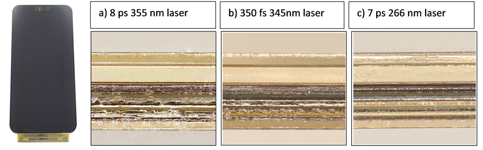
Under these higher demands, the process of record currently is shifting from UV picosecond lasers toward UV lasers with pulse durations in the 500-femtosecond range. While femtosecond lasers today have less energy available in the UV wavelength, Mmachining with shorter laser pulses allows a larger process window and has shown some improvement in production yield. However, there are strong indications that the cutting process will progress further using ultrashort pulse lasers with deep UV wavelengths (257 to 266 nm), which have yielded unparalleled quality for multiple materials. A recent study investigated a direct comparison of 355-nm picosecond, 345-nm femtosecond, and 266-nm picosecond lasers for cutting state-of-the-art OLED with a 14-layer full-stack (Fig. 1).1
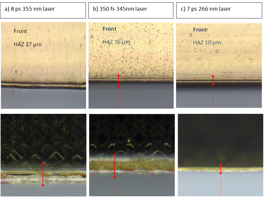
More important than the melt generation is the size of the heat affected zone (HAZ) on the front side and back side of the cut. Fig. 2 shows a comparison of this data for the best achieved results using the three different laser types. While operating at repetition rates below 1 MHz showed differences of almost a factor of 2, when processing at optimized parameters, the picosecond UV laser achieved almost an identical HAZ at the front side (Fig. 2a) and at the back side (Fig. 2b). The DUV picosecond laser showed the HAZ reduced by 40–60 percent across all repetition rates and scan speed compared to the UV picosecond and femtosecond lasers.
Deep UV Unlocks Cutting Quality and Efficiency
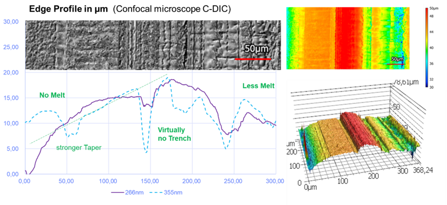
The edge profile of the cutting area of a full OLED display stack is measured with a confocal microscope (C-DIC). The solid purple line in Fig. 3 shows the profile for a cut with a DUV laser with virtually no melt and no void formation. In contrast, cutting with UV lasers (dashed line profile) often generates a trench in the middle of the stack that can be the starting point of delamination.
Optimum Pulse Duration and Wavelength
There are several process parameters beside the wavelength and pulse duration, e.g. cutting speed vs pulse repetition rate. Lower heat affected zones (less damages) can be seen at higher cutting speed and higher repetition rates. Fig. 4 compares the HAZ produced by UV femtosecond (343 nm) and UV picosecond (355 nm) lasers, showing that their results converge.
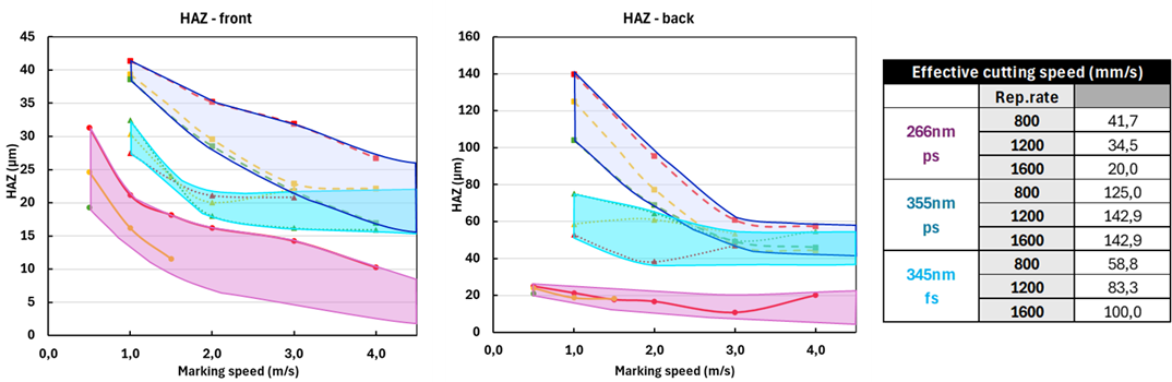
The quality improvement trend also can be observed for the DUV 266-nm picosecond cut. Overall, the HAZ is lower on both the entrance and exit sides. All three laser types in this test have different pulse energies and average powers available. The trend in Fig. 4. shows improved results for higher repetition rates and lower energies. The key finding, however, is that the normalized cutting efficiency (cutting speed per W) is similar for picosecond and femtosecond UV but almost a factor of 2 higher for DUV. Indicating that significantly less energy is used up by thermal and other damage effects. The current available DUV laser source has a maximum of 10 W, which is not sufficient for industrial throughput. Power scaling in the UV, especially in the DUV, is not trivial in the context with industrial-required laser lifetimes. There is a big difference in the laser architecture between picosecond and femtosecond lasers. This has a big impact on power scaling at the DUV level.
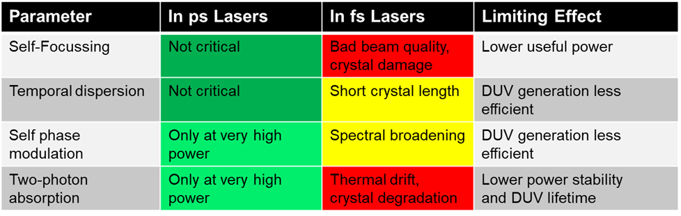
DUV generation in solid-state lasers uses the nonlinear optical (NLO) effect of harmonic generation in crystals. The required laser intensities are close to unwanted NLO, which compromises performance and strongly determines the design of a DUV laser. The listed laser parameters in Table 1 show the DUV picosecond laser would be the straightforward solution when it comes to industrial 24/7 display cutting.
Outlook
The next step to bring DUV into industrial OLED cutting is the power scaling of the available lasers, which currently have a typical DUV output power of 10 W. Although the cutting efficiency per Watt of DUV lasers is about a factor of 2 higher, when compared to UV lasers, this cannot compensate for the typically five times lower output power provided today. Deep UV lasers with power levels of 20 W and more are currently under development, and they could be a breakthrough for display manufacturing as well as for microelectronics in general.
Summary
UV picosecond and femtosecond lasers are essential for the cutting of mobile OLED displays at a certain quality level. The best results—lowest HAZ—were achieved with DUV 266-nm picosecond lasers. A laser power level of 20+ W is necessary to meet the industrial throughput requirements from display manufacturers. The use of DUV will be a big step forward and will improve the display quality and might overcome the potential delamination effect for foldable phones in the future.
Reference
1. Haupt, O., Soerensen, F., Knappe, R., & Belakowski, A. (2025). UV and DUV laser cutting of OLED displays for an enlarged active area. Laser-Based Micro- and Nanoprocessing XIX. Proceedings of SPIE Volume 13351. Laser Applications and Systems in Engineering, San Francisco, California. https://doi.org/10.1117/12.3040653