Ion Implantation for Semiconductor Devices
Coherent advanced ion implantation foundry services support semiconductor manufacturers from R&D through volume production.
November 8, 2023 by Coherent
Semiconductors, such as silicon, germanium, gallium arsenide, indium phosphide, gallium nitride and silicon carbide, are the basis of microelectronics technology. The element silicon alone is used in about 90% of the microchips made today.
As their name implies, semiconductors have limited electrical conductivity. But their conductivity can be increased by introducing other elements into their crystal lattices. This process is called doping. Performing this doping in a very precise and spatially selective manner is what enables the creation of useful circuit elements, like transistors, within a semiconductor substrate.
Since the early 1970’s, the most widely used method for semiconductor doping is ion implantation. Ion implantation enables microchip fabrication.
Despite the importance of ion implantation, manufacturers often outsource this process to external vendors. Notably, Coherent is the largest and longest-established ion implantation foundry service in the world. To understand why chipmakers large and small rely on Coherent for this vital process, let’s first learn a bit about ion implantation technology.
Ion Implantation Basics
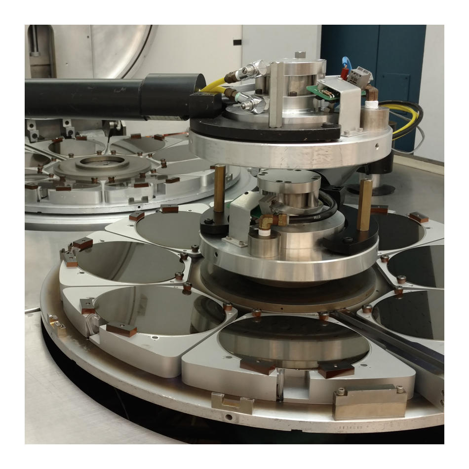
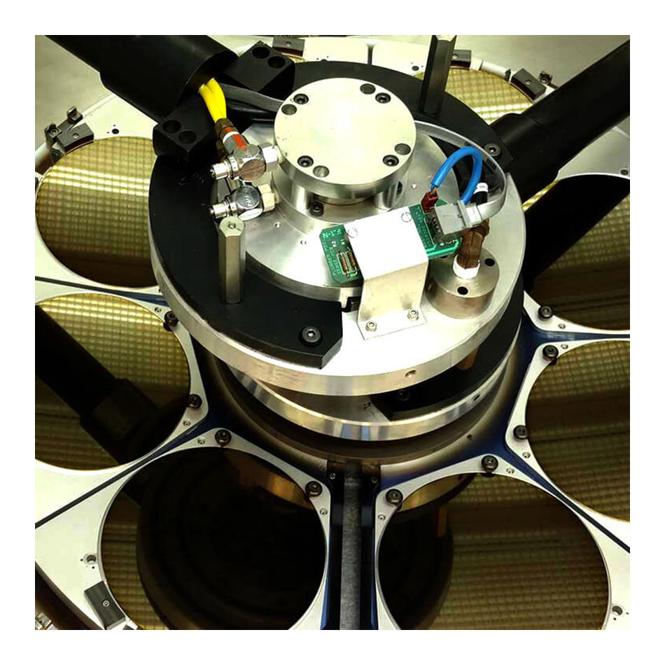
The heart of an ion implanter is the ion source. Here, electrons are stripped from atoms or molecules to make positive ions. The positive ions are then extracted from the ion source using a high-voltage electrostatic field to form the ion beam.
Next, the ion beam passes through a mass analysis module. This selectively separates out only the desired ions species required to modify the semiconductor material.
After mass analysis, the high-purity ion beam is focused and shaped. The conditioned ion beam is then accelerated to the desired energy and scanned uniformly across the semiconductor substrate.
The high-energy ions penetrate into the semiconductor material and embed themselves within its crystal lattice. This energetic implantation process also creates defects and damages the semiconductor crystal lattice. For some applications, this damage is beneficial and used to isolate areas on the chips and the integrated circuits.
For other applications, an annealing cycle (heating and cooling) is performed to repair this damage and “activate” the dopants. Specifically, heating the material enables implanted ions to move from where they’ve randomly lodged within the crystal to locations where they become incorporated into the lattice itself (substituting themselves for the original atoms). Dopant activation produces the desired increase in electrical conductivity of the material.

Outsourcing Ion Implantation
If the preceding description makes an ion implantation tool sound like a complex and sophisticated machine, that’s because it is. This complexity becomes even more pronounced when you consider all the control systems, process monitoring electronics, and computer hardware necessary to achieve the exceptional precision and consistency required for semiconductor manufacturing.
There are a few other important practical things to note about ion implantation tools. First, each tool is tailored to generate ions within a specific range of energies and dose (the amount of ions to incorporate into a material). They are also built to work with particular chemical species. There isn’t a one-size-fits-all ion implantation tool that can handle all possible applications.
Next, ion implantation tools can be big – like living room-sized big. Also, they require substantial specialized knowledge and expertise to run and maintain.
Finally, these tools come with a substantial price tag. Even the simplest ones can cost a few million dollars.
All of these characteristics often motivate even large-scale chipmakers to outsource ion implantation. Size alone is a significant factor because semiconductor fab floor space is limited, expensive, and at a premium. The production space occupied by a large ion implantation tool can often be utilized more cost-effectively by other systems, like a wafer stepper.
Outsourcing therefore allows manufacturers to limit capital expenditures and to focus on what they know best – like design or packaging. It frees them from the need to maintain specialized ion implantation expertise.
In addition to large commercial fabs, ion implantation foundries also service R&D groups, process development teams, and low-volume producers. In these cases, the production volumes don’t justify the investment in a dedicated tool. Moreover, for development purposes, it may not be feasible to find a single ion implantation tool with all the required capabilities. Additionally, a manufacturer might lack the in-house expertise to explore and implement a wide range of ion implantation strategies.

The Coherent Foundry
How did Coherent become the world’s premier ion implantation foundry? That journey actually began all the way back in 1976 when two different companies – the Implant Center and Ion Implant Services – were both formed in San Jose, California. These groups merged to become INNOViON in 2000 which was subsequently acquired by II-VI (now Coherent) in 2020. Today, Coherent operates three ion implantation foundries – two in the United States (San Jose and Wilmington, Massachusetts) and one in Hsinchu, Taiwan.
Our extensive history has allowed us to amass the most comprehensive set of production capabilities among ion implantation foundries. We operate a diverse array of over 30 ion implantation tools from all major manufacturers. This diversity enables us to accommodate virtually any combination of ion implantation parameters (energy, dose, temperature, etc.), species, wafer size, and substrate material.
In addition to our technical capabilities, our decades of operation have provided us with invaluable experience. Our dedicated staff collectively possesses several hundreds of man-years of wafer fabrication and process engineering experience. Beyond foundry services, we offer expertise that supports every facet of ion implantation technology, including integration consulting, simulations, and tooling development.
Our wide range of services positions Coherent to add value at every stage of the semiconductor product life cycle – from proof-of-concept to pilot line production, and all the way through to high volume outsourcing. That’s why the Coherent ion implantation foundries today serve over 200 commercial microelectronics manufacturers worldwide, as well as dozens of universities, governmental labs, and advanced R&D institutions.
But we’re not resting on our past successes. We’re also actively involved in developing new technology to support emerging materials. Probably the most important of these is silicon carbide (SiC). The unique characteristics of this wide-bandgap semiconductor require that both the implantation and annealing cycles be carried out at much higher temperatures than for traditional materials like silicon. Coherent has already incorporated “hot implant” capabilities into our foundry to specifically cater to SiC, demonstrating our commitment to staying at the forefront of technology.
Learn more about Coherent ion implantation foundry services.
Related Resources
By providing your information and clicking ‘Subscribe’, you opt-in to receiving periodic email marketing communications from Coherent Corp. and understand that your personal data will be processed in accordance with our Privacy Policy and that our Terms apply. You may opt-out of marketing emails sent by us at any time by clicking the unsubscribe link in any marketing email you receive.
